���һ��֣�![]()
Ӫҵִ�գ������
��Ӫģʽ��ó��/����/����
���ڵ������㶫 ����
��ҵ��վ��
http://qsd.dzsc.com
���֤����
��Ա���ͣ�
��Ա���ޣ�13��
������ 
�绰��0755-83264115
�ֻ���15889758566
18948336722
�绰��0755-82710921
�ֻ���13714022780
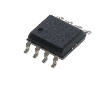
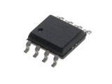
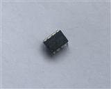

IR2102STRPBF
IR(����������)
DIP8
360 mA
20 V
10 V
- 40 C
+ 125 C
Features IR2102STRPBF IR2102STRPBF IR2102STRPBF IR2102STRPBF IR2102STRPBF
• Floating channel designed for bootstrap operation
Fully operational to +600V
Tolerant to negative transient voltage
dV/dt immune
• Gate drive supply range from 10 to 20V
• Undervoltage lockout
• 3.3V, 5V, and 15V logic input compatible
• Matched propagation delay for both channels
• Outputs in phase with inputs (IR2101) or out of
phase with inputs (IR2102)
• Also available LEAD-FREE
HIGH AND LOW SIDE DRIVER
Product Summary
VOFFSET 600V max.
IO+/- 130 mA / 270 mA
VOUT 10 - 20V
ton/off (typ.) 160 & 150 ns
Delay Matching 50 ns
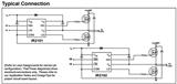
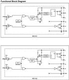
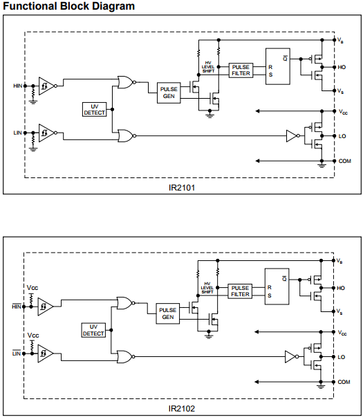
IR2101(S)/IR2102(S) & (PbF)
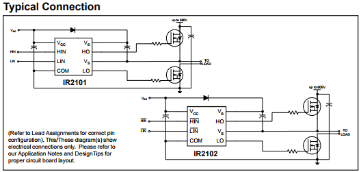
Description
The IR2101(S)/IR2102(S) are high voltage, high speed
power MOSFET and IGBT drivers with independent
high and low side referenced output channels. Proprietary
HVIC and latch immune CMOS technologies
enable ruggedized monolithic construction. The logic
input is compatible with standard CMOS or LSTTL
output, down to 3.3V logic. The output drivers feature a high pulse current buffer stage designed for minimum
driver cross-conduction. The floating channel can be used to drive an N-channel power MOSFET or IGBT in
the high side configuration which operates up to 600 volts.
Symbol Definition Min. Max. Units
VB High side floating supply voltage -0.3 625
VS High side floating supply offset voltage VB - 25 VB + 0.3
VHO High side floating output voltage VS - 0.3 VB + 0.3
VCC Low side and logic fixed supply voltage -0.3 25
VLO Low side output voltage -0.3 VCC + 0.3
VIN Logic input voltage (HIN & LIN) -0.3 VCC + 0.3
dVS/dt Allowable offset supply voltage transient �� 50 V/ns
PD Package power dissipation @ TA �� +25��C (8 lead PDIP) �� 1.0
(8 lead SOIC) �� 0.625
RthJA Thermal resistance, junction to ambient (8 lead PDIP) �� 125
(8 lead SOIC) �� 200


 ѯ��
ѯ��