- 非IC关键词
企业档案
- 相关证件:

- 会员类型:普通会员
- 朱亮成

- 电话:0755-83264115
- 手机:15889758566
- 18948336722
- 电话:0755-82710921
- 手机:13714022780
- 地址:深圳市福田区华强北赛格科技园四栋中12楼A4座―2L
- 传真:0755-83955172
- E-mail:1282971461@qq.com
产品分类


 询价
询价产品信息
制造商:ON Semiconductor
厂家:ONSEMI [ON Semiconductor]
描述:Complementary Darlington Power Transistors
产品种类:Transistors Darlington
配置:Single
晶体管极性:NPN
集电极―发射极电压 VCEO:100 V
发射极 - 基极电压 VEBO:5 V
集电极―基极电压 VCBO:100 V
直流电集电极电流:2 A
集电极截止电流:20 uA
功率耗散:20 W
工作温度:+ 150 C
安装风格:SMD/SMT
封装 / 箱体:TO-252-3 (DPAK)
封装:Tube
集电极连续电流:2 A
直流集电极/Base Gain hfe Min:200, 500, 1000
工作温度:- 65 C
工厂包装数量:75
特点:
•无铅包可用
•铅形成在塑料套管表面贴装应用(没有后缀)
•直引线型的塑料套管( “-1”后缀)
•铅16毫米磁带和卷轴形成版本( “ T4 ”和“ RL ”后缀)
•电类似于热门TIP31和TIP32系列
Features
• Lead Formed for Surface Mount Applications in Plastic Sleeves
(No Suffix)
• Straight Lead Version in Plastic Sleeves (“−1” Suffix)
• Electrically Similar to Popular TIP31 and TIP32 Series
• NJV Prefix for Automotive and Other Applications Requiring
Unique Site and Control Change Requirements; AEC−Q101
Qualified and PPAP Capable
• These Devices are Pb−Free and are RoHS Compliant*
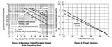
MJD112 (NPN), MJD117 (PNP)
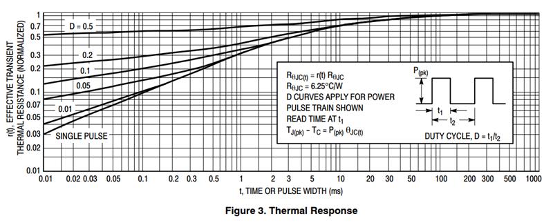
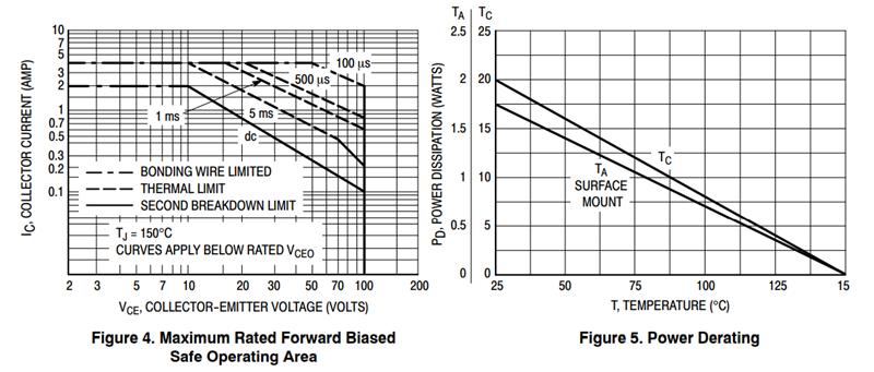
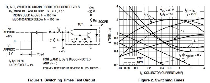
There are two limitations on the power handling ability of
a transistor: average junction temperature and second
breakdown. Safe operating area curves indicate IC − VCE
limits of the transistor that must be observed for reliable
operation; i.e., the transistor must not be subjected to greater
dissipation than the curves indicate.
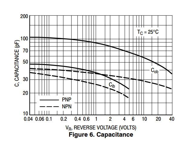
The data of Figures 5 and 6 is based on TJ(pk) = 150C; TC
is variable depending on conditions. Second breakdown
pulse limits are valid for duty cycles to 10% provided
TJ(pk) < 150C. TJ(pk) may be calculated from the data in
Figure 4. At high case temperatures, thermal limitations will
reduce the power that can be handled to values less than the
limitations imposed by second breakdown.C