相关证件:
会员类型:
会员年限:14年
朱亮成 
电话:0755-83264115
手机:15889758566
18948336722
电话:0755-82710921
手机:13714022780
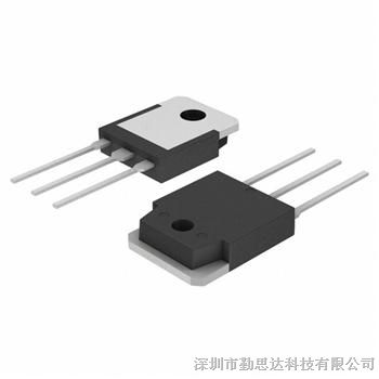
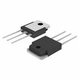


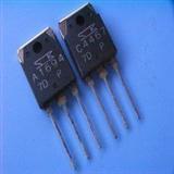
The NJW21193G and NJW21194G utilize Perforated Emitter
technology and are specifically designed for high power audio output,
disk head positioners and linear applications.
Features
• Total Harmonic Distortion Characterized
• High DC Current Gain
• Excellent Gain Linearity
• High SOA
• These Devices are Pb−Free and are RoHS Compliant
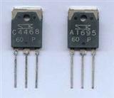
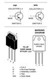
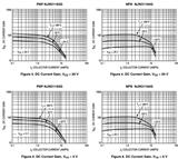
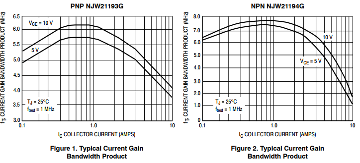
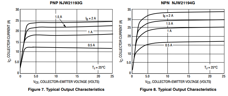
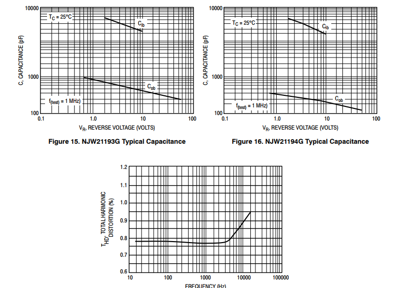
NJW21193G (PNP) NJW21194G (NPN)
 NJW21193G (PNP) NJW21194G (NPN)
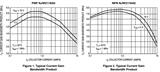
The data of Figure 13 is based on TJ(pk) = 150°C; TC is
variable depending on conditions. At high case
temperatures, thermal limitations will reduce the power than
can be handled to values less than the limitations imposed by
second breakdown.
There are two limitations on the power handling ability of
a transistor; average junction temperature and secondary
breakdown. Safe operating area curves indicate IC − VCE
limits of the transistor that must be observed for reliable
operation; i.e., the transistor must not be subjected to greater
dissipation than the curves indicate.


 询价
询价