收藏本公司 人气:1232213
逻辑IC(1)
LDO(2)
稳压IC(1)
充电管理IC(1)
其他电源IC(9)
整流二极管(1)
MOSFET(2)
霍尔传感器(1)
光电光耦合器(光耦)(1)
其他(1)
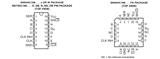
SN74HC166N
TI(德州仪器)
Serial/Parallel to Serial
1
8
5 / 3
150 ns, 30 ns, 26 ns
6 V
- 40 C
+ 85 C
3
点击下载PDF


 询价
询价