相关证件:
会员类型:
会员年限:14年
朱亮成 
电话:0755-83264115
手机:15889758566
18948336722
电话:0755-82710921
手机:13714022780


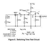
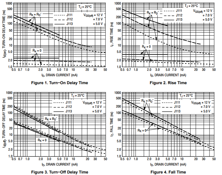
The switching characteristics shown above were measured using a test
circuit similar to Figure 5. At the beginning of the switching interval,
the gate voltage is at Gate Supply Voltage (−VGG). The Drain−Source
Voltage (VDS) is slightly lower than Drain Supply Voltage (VDD) due
to the voltage divider. Thus Reverse Transfer Capacitance (Crss) or
Gate−Drain Capacitance (Cgd) is charged to VGG + VDS.
During the turn−on interval, Gate−Source Capacitance (Cgs)
discharges through the series combination of RGen and RK. Cgd must
discharge to VDS(on) through RG and RK in series with the parallel
combination of effective load impedance (R′D) and Drain−Source
Resistance (rds). During the turn−off, this charge flow is reversed.
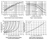
Predicting turn−on time is somewhat difficult as the channel resistance
rds is a function of the gate−source voltage. While Cgs discharges, VGS
approaches zero and rds decreases. Since Cgd discharges through rds,
turn−on time is non−linear. During turn−off, the situation is reversed
with rds increasing as Cgd charges.


 询价
询价