供应24LC02BT-I/OT储存器 可擦除可编程
Features • Single Supply with Operation down to 1.7V for 24AA02 and 24FC02 Devices, 2.5V for 24LC02B Devices • Low-Power CMOS Technology: - Read current 1 mA, maximum - Standby current 1 μA, maximum (I-temp.) • 2-Wire Serial Interface, I2C Compatible • Schmitt Trigger Inputs for Noise Suppression • Output Slope Control to Eliminate Ground Bounce • 100 kHz, 400 kHz and 1 MHz Compatibility • Page Write Time: 5 ms, Maximum • Self-Timed Erase/Write Cycle • 8-Byte Page Write Buffer • Hardware Write-Protect • ESD Protection >4,000V • More than 1 Million Erase/Write Cycles • Data Retention >200 Years • Factory Programming Available • RoHS Compliant • Temperature Ranges: - Industrial (I): -40°C to +85°C - Extended (E): -40°C to +125°C • Automotive AEC-Q100 Qualified
Description The Microchip Technology Inc. 24XX02(1) is a 2-Kbit Electrically Erasable PROM. The device is organized as one block of 256 x 8-bit memory with a 2-wire serial interface. Its low-voltage design permits operation down to 1.7V with standby and active currents of only 1 μA and 1 mA, respectively. The 24XX02 also has a page write capability for up to 8 bytes of data.
供应24LC02BT-I/OT 24LC02BT-I/OT 24LC02BT-I/OT 24LC02BT-I/OT
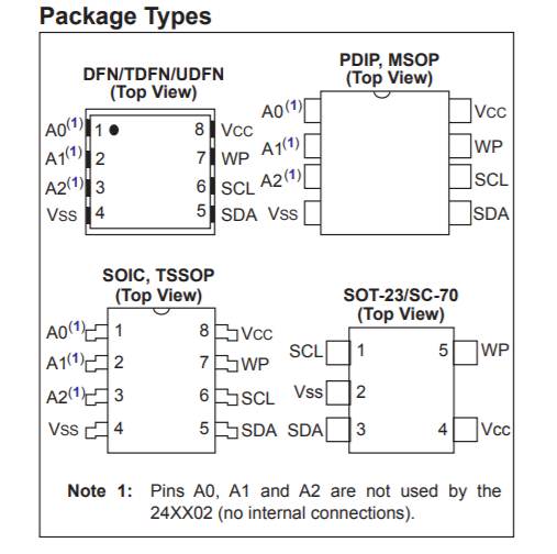
 Packages
• 8-Lead DFN, 8-Lead MSOP, 8-Lead PDIP,
8-Lead SOIC, 8-Lead TDFN, 8-Lead TSSOP,
8-Lead UDFN, 5-Lead SOT-23 and 5-Lead SC-70
Description The Microchip Technology Inc. 24XX02(1) is a 2-Kbit Electrically Erasable PROM. The device is organized as one block of 256 x 8-bit memory with a 2-wire serial interface. Its low-voltage design permits operation down to 1.7V with standby and active currents of only 1 μA and 1 mA, respectively. The 24XX02 also has a page write capability for up to 8 bytes of data.

Random read operations allow the master to access any memory location in a random manner. To perform this type of read operation, the word address must first be set. This is accomplished by sending the word address to the 24XX02 as part of a write operation. Once the word address is sent, the master generates a Start condition following the acknowledge. This terminates the write operation, but not before the internal Address Pointer is set. The master then issues the control byte again, but with the R/W bit set to a ‘1’. The
